My 2019-era Dell laptop died recently, a few days after I’d replaced the battery. More specifically, the laptop was still running fine off the battery but it had lost its ability to charge from the mains. Without any way to recharge the battery, the laptop was useless.
The green LED on the charger would just turn off when I plugged it into laptop, and the laptop did not detect a charger. The charger itself was fine – I measured the expected 19.5v when the green LED was on, but 0v after plugging it into the laptop. This was clearly bad news, but with a small glimmer of hope. The charger was clearly detecting a short and shutting down (nice safety measure). Perhaps it was just the laptop power jack that was shorted? Unfortunately not – I opened up the laptop, removed the jack and its motherboard cable and that part wasn’t shorted. I could even put the liberated jack/cable assembly onto the power supply and the green LED happily stayed on.
The short was clearly on the motherboard itself – quickly confirmed with a continuity check on the motherboard connector – 0.2ohms. However, the fact that the laptop ran off the battery meant that the fault must be isolated to the charging section only – another glimmer of hope.
Fortunately, the badcaps website had both a circuit diagram and a CAD/layout file for my laptop model.
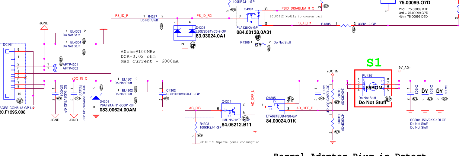
On the left is the power connector, with grounds at the top and power at the bottom. The 19.5v rail has a 10uF cap smoothing cap, a couple of 1uF’s and a zener diode to stabilize the voltage. This is all pretty vanilla so far. Next there’s a big mosfet switch, whose gate is controlled by some ‘AC DISABLE’ line. But crucially, this mosfet helped narrow down the fault since it’s open when the laptop is powered down. Prodding around with the continuity meter showed that everything to the left of the mosfet was shorted, whereas everything on the right was fine. So now we’ve narrowed the suspects down to 3 caps and 1 zener diode. If I had to bet, I’d guess it would be the 10uF cap, since 10uF is a lot of capacitance to fit into a tiny 0603 ceramic cap and must require lots of super-thin dielectric layers. But we need more than a guess.
The badcaps site also had a .cad file. What format is .cad? Fortunately it was a simple textual format containing a comment “USER MENTOR GRAPHICS” which was enough to identify it as GenCad format. And happily the latest version of OpenBoardViewer can read GenCad and display the layout. (It’s a 2 sided board, and it took me a while to realise that hitting spacebar flips to show the other side!).
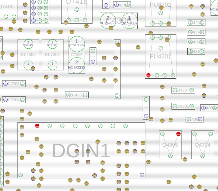
This shows the power connector (DCIN1), and the 10uF cap just above it (EC4301).
How to tell which component has shorted? If all the current is going through a shorted cap, it should be getting hot. I have a current-limited bench PSU, so I set it to max 1A, hooked up ground and then .. very carefully .. used a sharp multimeter probe to apply 1V to the right hand pins of the DCIN connector (this rail normally gets 19.5v so 1v is safe). As expected, the current limiter kicked in. I left it powered up for a few seconds, then used my finger to check if any of the caps or diodes were hot – but nothing obvious.
Next, I tried a more sensitive method – spread some isopropyl alcohol to wet all the nearby components, power up the circuit, and watch carefully to see if the IPA evaporates quickly from any one place. First few attempts were flops, then eventually I built up the courage to send 2A and then 3A through the board. At 3A, it became clear that the 10uF cap and the circuit board near it was drying up quickly, whereas the zeners and mosfets stayed wet. Success – we’ve identified which component is shorted! (an IR camera would’ve also been useful, but they’re pricey and I don’t have one).
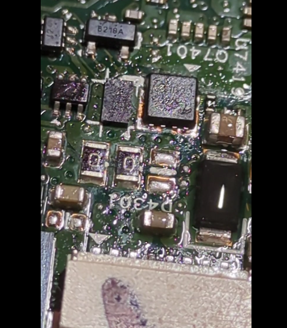
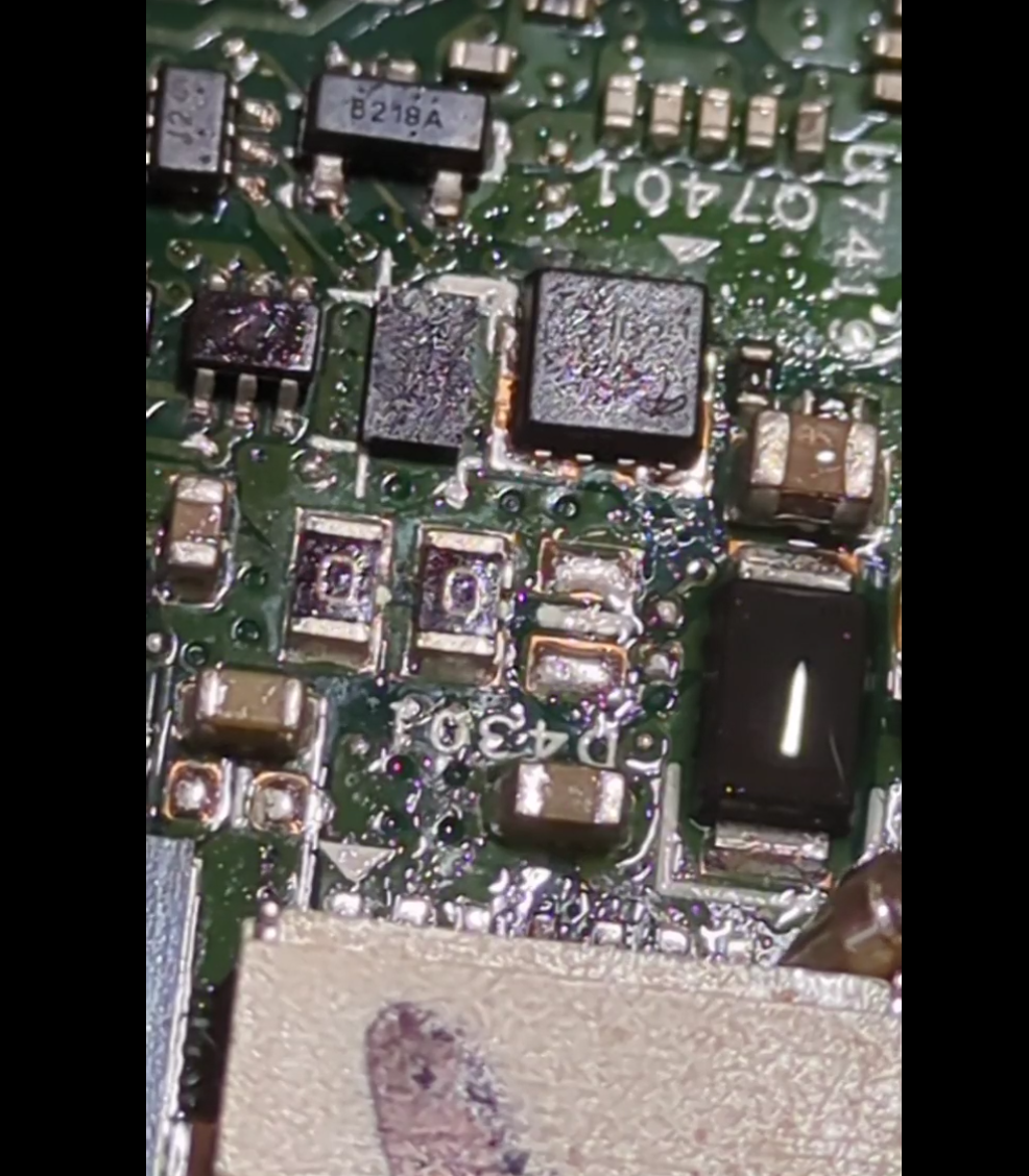
(In the left/before photo, the brown cap in the bottom-middle and the black zener diode are wet. In the right/after photo, the brown cap has dried whereas the black zener is still wet).
Up to this point, I have done SMD soldering exactly once in my life – building a ‘practice kit’ where you soldered 50 tiny SMD resistors to make a dummy load of radio testing. So the idea of trying to remove this failed 10uF from a laptop was somewhat scary. It’s 1.5mm long, and next to lots of even smaller components. But I figured there was a 50/50 chance of success, and so it was rational to ‘invest’ up to 50% of the value of the laptop in tooling (!) and so I acquired a hot-air rework station.
Being keenly aware that any mistake would fry the laptop, I also bought a couple of cheap “SMD practice kits” where you solder some 555s and decade counters and a heap of resistors, diodes, LEDs and transistors to make a pointless flashy light thing. After a few evenings practising, I felt like I had figured out the right temperature + airflow settings, as well as how to use solder paste and tweezers and magnification. When the hot-air works, it’s amazing – the solder melts and surface tensions pulls the component neatly into position. But I also learned to loathe SMD 1N4148 diodes, which are cylindrical and inevitably roll away, arg. The practice kit also says (in Chinese) that some components are deliberately defective, in order to let you “practice debugging as well as soldering”. I suspect ALL the components are rejects, and the fact that any of them worked is a miracle. In the end, the 4017 counter was fried but everything else worked. I desoldered and resoldered the 4017 several times to debug the problem, which was just more useful practice. In the end, 375C and 10% flow works well for soldering, but desoldering needs 30-40% flow so you can get one component hot quickly.
Youtube is amazing for learning new skills – this video in particular highlighted the value of using aluminium tape as temporary heat shielding, a brilliant idea. Most youtubers use pricey digital microscopes when working on SMDs. I mostly made do with cheap jewelers loupes, but at one point I was taking photos of the motherboard and I realised my phone (pixel 7a) was capable of acting as a digital microscope. I reused a camera clamp mount I already had, and hey presto – instant digital microscope for no additional outlay!
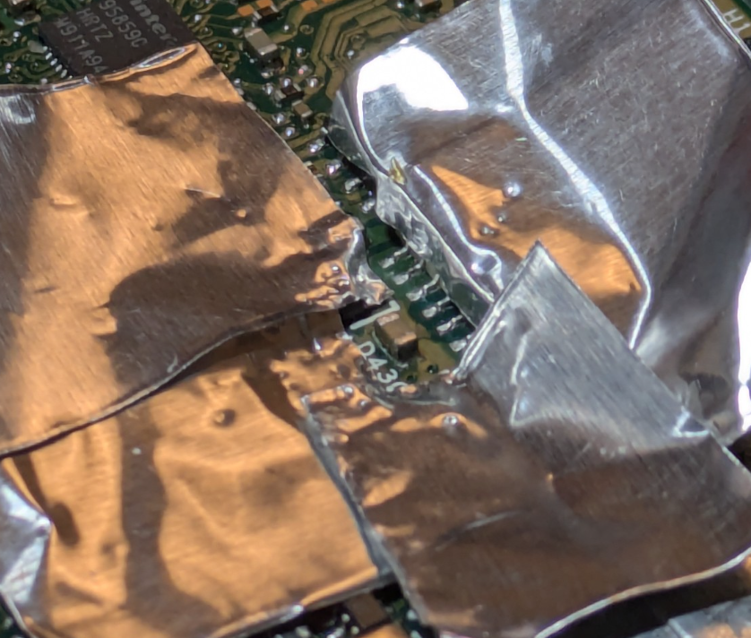
Finally, it was time for laptop surgery. I used the aluminium tape to isolate the failed cap – protecting the plastic power connector and covering nearby SMD components to try and stop them melting + blowing away.
Then I applied flux, held the cap with tweezers and applied heat and … nothing happened.
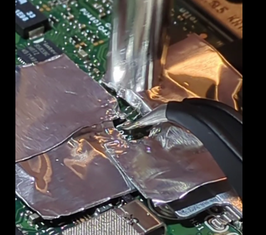
The cap felt like it was glued down. I tried again, keeping the heat on for much longer than I’d ever needed before. Still no movement. I tried increasing the temperate and airflow from 350 to 375C. Still no joy. Maybe the cap really was glued down? Maybe when it shorted it somehow stuck itself to the motherboard?
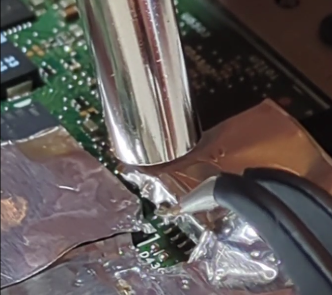
I tried switching back to my fine-tipped soldering iron, switching from one side to the other to try and get both sides molten and perhaps flick it out of position. Again, no joy. Then I remembered another youtube tip of adding some extra (leaded) solder to hopefully reduce the melting point of the existing likely lead-free stuff. But it still wouldn’t shift.
This was completely unlike the practice boards. On the practice boards, the components heated up quickly, the solder very visibly melted and it was easy to lift them off with tweezers. What could be different? I realised that the answer is that the laptop has a huuge ground plane – and all that mass of copper was just sucking the heat away quickly.
Nothing ventured, nothing gained .. so I turned up the temperature to 400C and 30% air, added more flux, and heated. And heated. And heated. And then – miracle of miracles, the solder melted and the capacitor lifted free!
After a week and a half of build up, this was the mugshot:
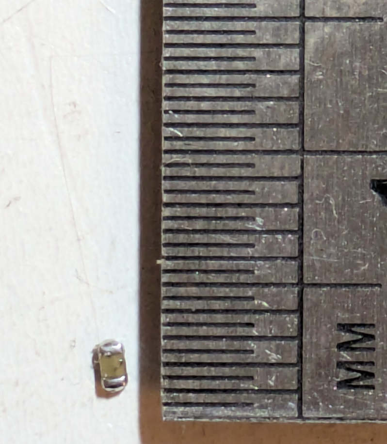
All that work for a 1.5mm long 0603 10uF capacitor. Resistance: 0 ohms. More of a “conductor” than a capacitor.
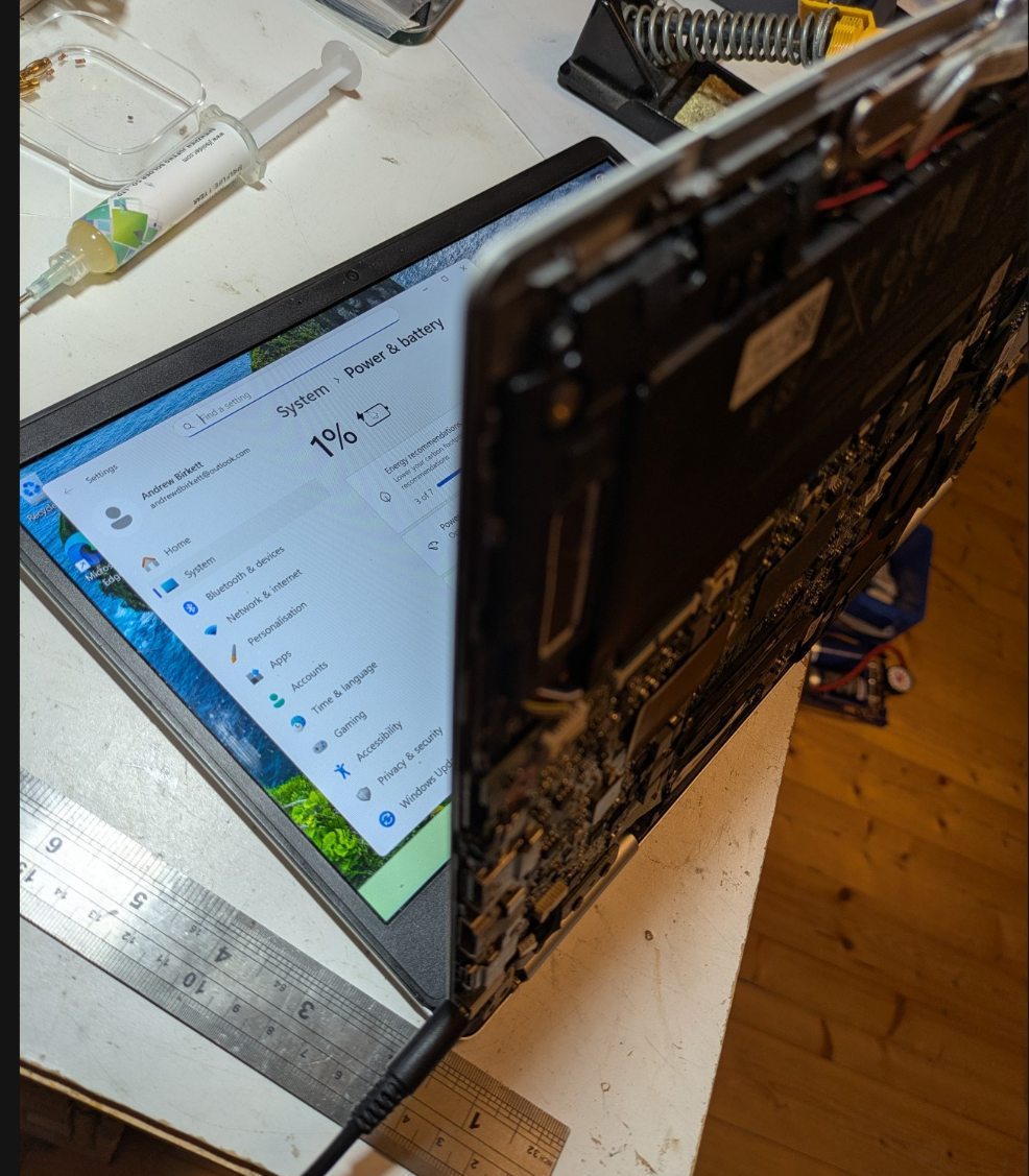
A quick check with the multimeter showed that the power line was no longer shorted. The mains charger kept its green LED of happiness on, and the laptop battery went from 0% charge to 1% charge quickly. Success!!
So all that remains is to get a replacement 10uF 25V capacitor and solder it in. The laptop works fine without it, at least in the short term. Internally, the 19.5v just gets stepped down to 12v, 5v, 3.3v etc anyway. But the designers presumably want the incoming power to be as smooth as possible, so I replaced it like-for-like.
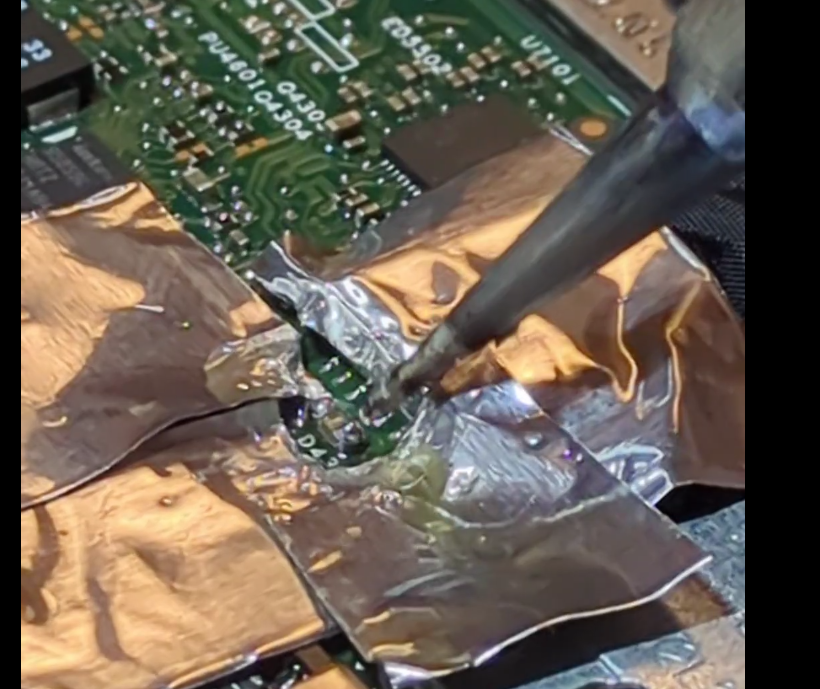
Preparing the pads for the new capacitor was an adventure. I initially tried cleaning the pads with solder braid and my soldering iron’s finest tip. But the soldering iron just stuck itself to the board! I quickly realised that the big ground plane was winning a tug’o’war with my 25W soldering iron, sucking all the heat away and causing the solder at the tip to solidify! Switching to the biggest tip solved the problem, although now it was super fiddly to manoeuvre the iron into place without bumping other components.
Soldering the cap into place was similar to the desoldering operation. Aluminium foil everywhere! I added a bit too much solder paste which balled up on the pads. I initially held the new capacitor with tweezers in the molten solder and let it cool. However, the cap ended up looking “high up” on the board. A second pass just using hot air at 20% flow remelted the solder, and the capacitor sunk down and nicely aligned itself.
A continuity check showed that we had a clean connection to ground on one side, and to the power rail on the other end. I had also measured the capacitance between ground + power beforehand at 0.17uF, and this went up to 3.9uF with the new cap. I was expecting 2uF before and 12uF afterwards, but I suppose the zener diode or other components might be messing with my capacitance readings? Regardless, there was a clear increase in capacitance which gave me confidence that the new capacitor was working.
A successful outcome! One laptop saved.